Paid
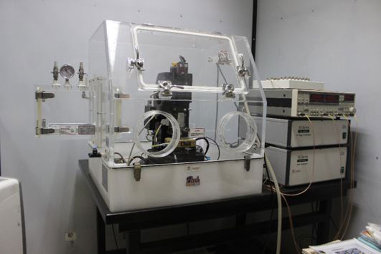
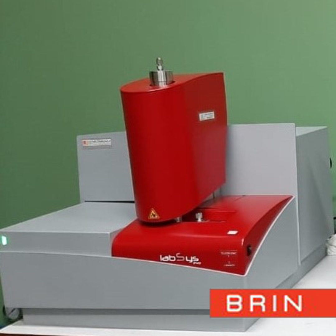
SERVICE DESCRIPTION | Scanning Electron Microscope (SEM) is a type of electron microscope that produces an image of a sample by scanning a surface with a focused electron beam with magnification up to a certain scale. The electrons interact with the atoms in the sample, generating…
- IBBN - Laboratorium Uji IRM - Teknologi Bahan Bakar Nuklir
- KST Serpong (Bacharuddin Jusuf Habibie)
Kawasan BJ. Habibie Gedung 20, Setu, Tangerang Selatan, BANTEN - 081110646763
- dit-pfk@brin.go.id
Marketing Office
Deputi Bidang Infrastruktur Riset dan Inovasi BRIN
layanan_sains@brin.go.id
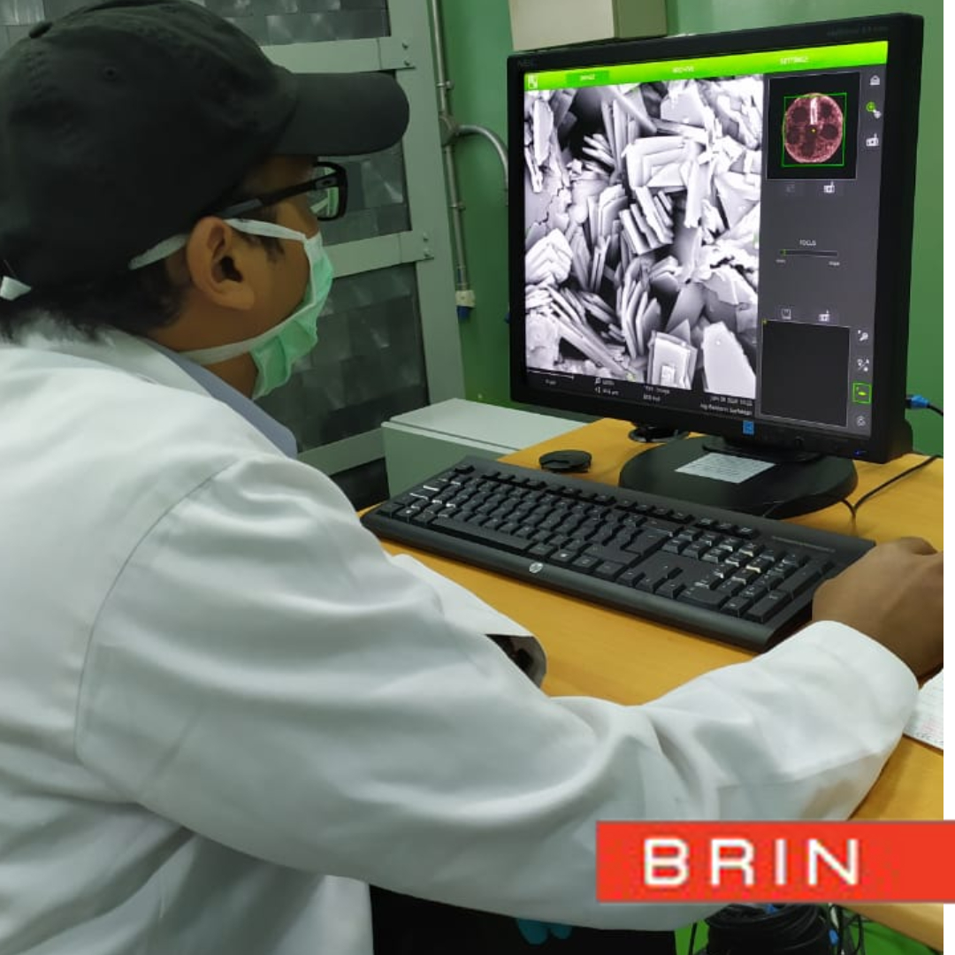
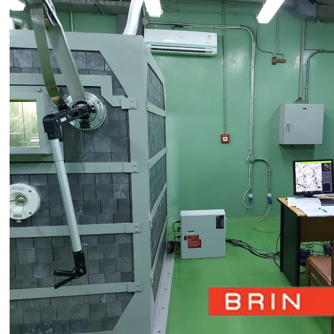
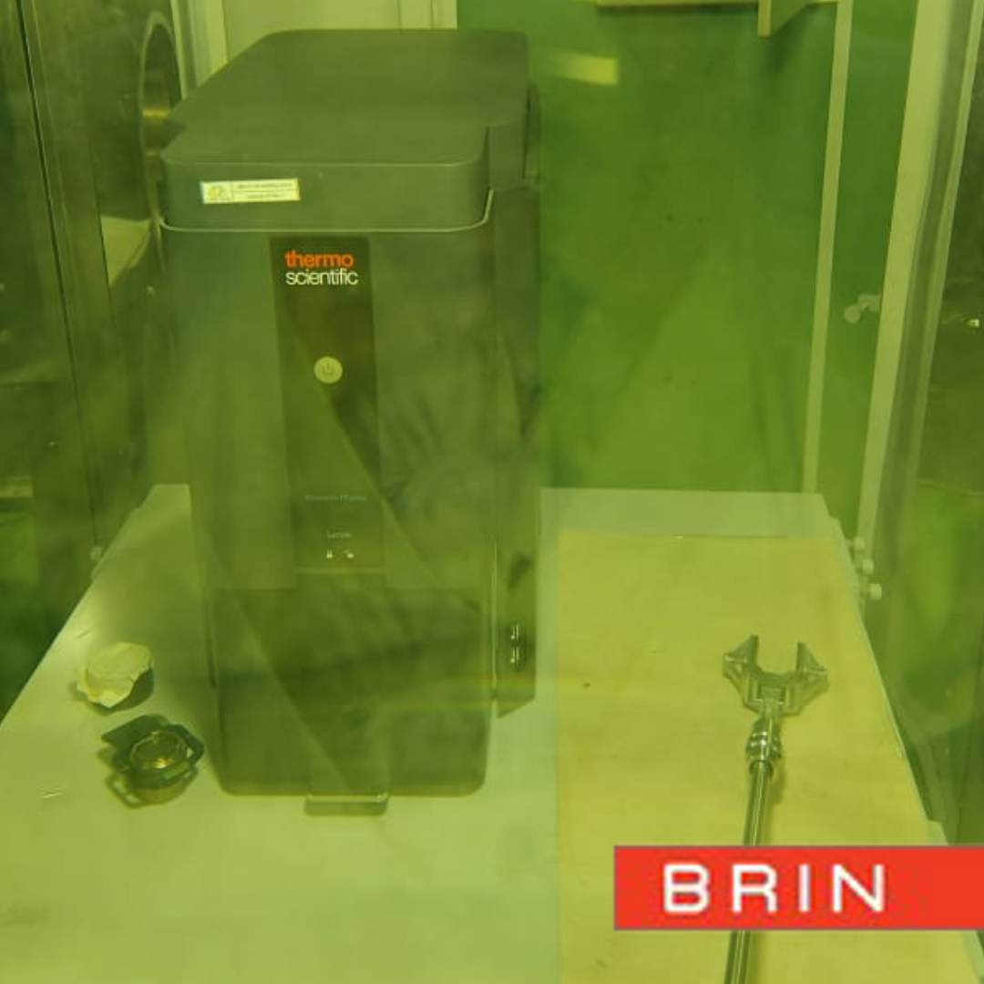
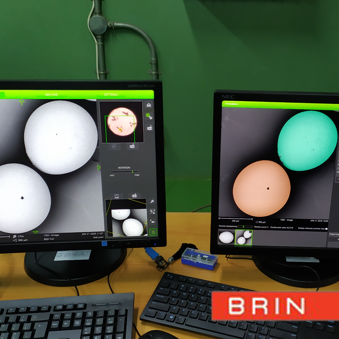
Scanning Electron Microscope (SEM) is a type of electron microscope that produces an image of a sample by scanning a surface with a focused electron beam with magnification up to a certain scale. The electrons interact with the atoms in the sample, generating various signals that contain information about the surface topography and composition of the sample.
For each sample package, Customers get the opportunity to take 3 image points (one of the best image magnification each) or one sample point but there are three best image magnification scales) with Backscattered electron detector (BSD) and Secondary electron detector (SED).
The sample is in the form of powder or solid which has a flat surface with dimensions of 2 cm and a thickness of < 2>
This service is only a testing service, for preparation in the form of gold plating, please apply to the "Gold Plating for SEM & EDS Testing" service.
Application Requirements:
- Photo
- Other Supporting File
| File Name | File Size | |
|---|---|---|
| Service SOP file | 0.15 MB | |
| Template Photo | 0 MB | |
| Template Other Supporting File | 0 MB |


